
Fab processes that enable stacked transistors, hybrid bonding, and advanced packaging are driving the need for more and better measurements.
The Challenges of 3D Metrology and Inspection in Advanced Nodes
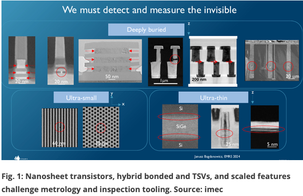
As semiconductor technology advances into 3D architectures and sub-2nm nodes, metrology and inspection tools face unprecedented challenges. Key issues include detecting buried defects, increasing feature sensitivity, and controlling process variability. Novel structures like CFETs, 3D-ICs, and hybrid bonding require new inspection methods to meet tighter tolerances. Optical and SEM-based tools are still widely used. However, they are showing their limitations, prompting the adoption of advanced techniques like X-ray diffraction and voltage contrast for buried defect detection. Techniques like scatterometry are evolving to handle complex nanosheet transistors, while hybrid bonding calls for precise copper pad measurement using interferometry and AFM (Atomic Force Microscopy).
Data Analytics: The New Frontier for Yield Optimization
With the increasing complexity of chip designs, advanced fabs are integrating AI-driven analytics platforms to enhance precision and accelerate process ramp-ups. These platforms sift through vast amounts of data to identify critical issues faster and more accurately. Yield management systems use machine learning to improve the correlation between metrology results and process outcomes, reducing defects and optimizing manufacturing efficiency. Tools like ASML YieldStar, Siemens’ Calibre SONR, and PDF Solutions’ FIRE platform are pioneering these advancements, helping fabs tackle random and systematic defects at advanced nodes like 3nm and pushing the limits of yield learning and defect identification.
My Take
As semiconductor complexity grows, integrating advanced data analytics and machine learning will be essential for keeping pace with shrinking nodes and novel architectures. The future of metrology lies in the ability to make sense of massive data sets quickly and accurately. However, the key differentiator for fabs will be how seamlessly they integrate these analytics platforms with real-time feedback into their manufacturing processes, ensuring continuous optimization and faster yield ramp-ups.
#Semiconductors #Metrology #DataAnalytics #AI #AdvancedManufacturing #EUV #3DNAND #CFET #ChipDesign #MachineLearning
Link to article:
https://semiengineering.com/metrology-advances-step-up-to-sub-2nm-device-node-needs/
Credit: Semiconductor Engineering