
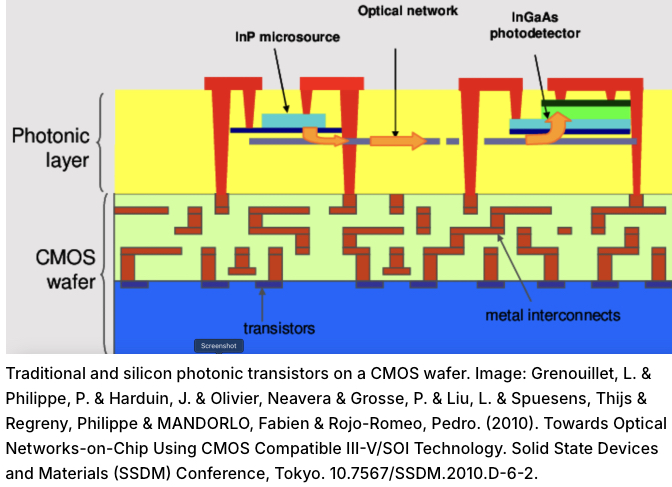
NVIDIA and TSMC reportedly developed a groundbreaking silicon photonics-based chip prototype at the end of last year, blending photonic circuits with traditional ones to tackle the limitations of semiconductor fabrication. Silicon photonics replaces electrons with photons for communication within chips, enabling faster data speeds and higher bandwidth without requiring ultra-advanced manufacturing techniques. This innovation comes alongside their work on optoelectronic integration and advanced packaging technologies, addressing critical constraints in AI chip performance, cost, and supply. As TSMC remains NVIDIA’s primary manufacturing partner, this collaboration underscores their push to overcome scaling challenges and redefine AI chip capabilities.
My Take
Silicon photonics can potentially redefine Moore’s Law for the AI era, focusing on architectural innovation rather than just transistor density. This shift could unlock new possibilities for edge computing and AI applications, driving unprecedented efficiency in data processing. Silicon photonics can deliver 10–50x higher bandwidth and up to 90% lower power consumption for data transfer.
#NVIDIA #TSMC #SiliconPhotonics #AIChips #Semiconductors #AdvancedPackaging #Innovation #TechnologyLeadership
Link to article:
https://wccftech.com/nvidia-tsmc-develop-advanced-silicon-photonic-chip-prototype-says-report/amp/
Credit: Wccftech
This post reflects my own thoughts and analysis, whether informed by media reports, personal insights, or professional experience. While enhanced with AI assistance, it has been thoroughly reviewed and edited to ensure clarity and relevance.