
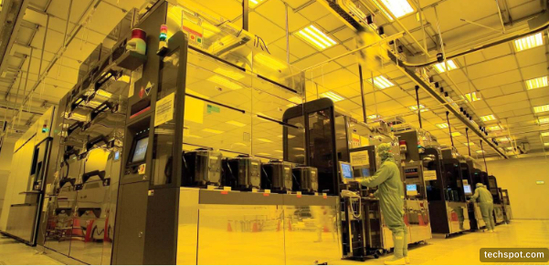
Executive Summary: TSMC is pushing chip production below 1nm, a milestone that will concentrate the world’s most advanced AI compute capacity into a small number of ultra-capital-intensive fabs.
Sub-1nm production forces semiconductor scaling into the Atomic Scaling Barrier, where transistor density gains depend less on lithography cadence and more on materials engineering, backside power delivery, and advanced packaging integration. TSMC converts scaling into a system-level discipline, tying compute performance to tightly coupled fabrication, memory proximity, and energy efficiency. This consolidates control over the compute layer, as only a handful of players can finance the tens of billions required per node while sustaining yield. The competitive landscape narrows to those who can co-design chips with manufacturing from day one, embedding customers deeper into foundry ecosystems.
“Below 1nm, shrinking transistors is no longer enough; performance is driven by how tightly chips, memory, and power systems are integrated.”
Prediction:
By 2029, at least two hyperscalers will commit >$10B each to co-designed nodes with TSMC, locking multi-year capacity at sub-1nm.
Foundry access will be allocated by strategic alignment, not just volume demand.
Note: TSMC is not targeting a specific number like 0.8 nm; “below 1 nm” refers broadly to the next generation beyond ~1.4 nm where node names become less precise and scaling depends more on system-level integration than transistor size alone.
hashtag#AIInfrastructure hashtag#ComputeInfrastructure hashtag#SemiconductorIndustry hashtag#ManufacturingScale hashtag#EnterpriseAI hashtag#SupplyChain hashtag#TechStrategy hashtag#IndustrialAutomation
Credit perplexity
https://www.perplexity.ai/page/tsmc-targets-sub-1nm-chip-prod-V2EFXl.mQC60WvbExCn8hw