
Executive Summary: Samsung Electronics 2nm yield plateau at ~55% establishes manufacturing precision as the gating factor for AI compute scaling, tightening control over advanced-node supply.
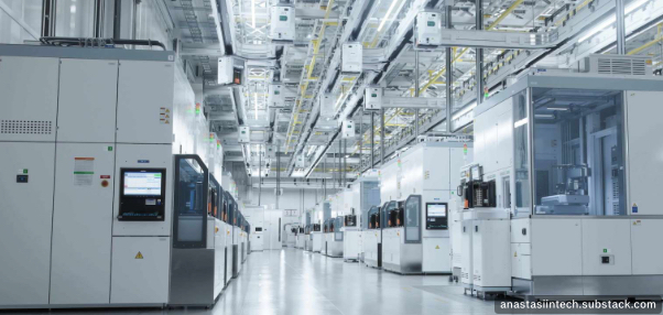
Samsung’s 2nm yield holding near 55% exposes the Yield-Control Barrier, where defect density, EUV variability, and process integration determine usable wafer output more than design ambition. At this level, nearly half of produced chips fail economic viability, directly constraining high-performance compute supply. This converts leading-edge manufacturing into a control layer of Intelligence Infrastructure, where only fabs achieving ≥70% yield unlock scalable AI deployment economics.
“At 2nm, yield defines power, not design.”
The consequence is structural: capacity leadership consolidates around players with stable high-yield nodes, tightening ecosystem dependency and raising the cost of competitive parity across AI infrastructure.
Prediction: By 2027, advanced-node capacity will consolidate around TSMC and one qualifying challenger, if a second supplier achieves ≥70% yield.
hashtag#AIInfrastructure hashtag#ComputeInfrastructure hashtag#SemiconductorIndustry hashtag#ManufacturingScalehashtag#EnterpriseAI hashtag#SupplyChain hashtag#TechStrategy hashtag#IndustrialAutomation
Credit perplexity
https://www.perplexity.ai/page/samsung-s-2nm-chip-yields-stuc-le9wh6yLR3eQl4PtbDt88Q